One of the most important fabrication methods for semiconductor applications is epitaxy, the growth of an oriented single crystal film on a substrate. This is termed heteroepitaxy when a film of one material is grown on a different substrate material. Regarding electronic materials performance, there are many benefits to growing different materials on top of each other, but a major side effect of heteroepitaxial growth processes is lattice mismatch. It can be quantified by
\[\epsilon_{misfit}=\frac{a_{f}-a_{s}}{a_{s}}\]
where \(a_{f}\) and \(a_{s}\) are the lattice constants between the film layer and the substrate, respectively, and \(\epsilon_{misfit}\) is the lattice mismatch strain. Because of this effect, formation of a flat layer may not be energetically favorable, even if it lowers the surface energy. Varying amounts of lattice mismatch can result in three different growth modes:
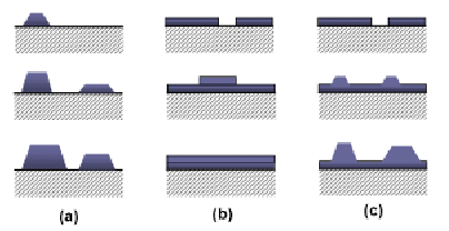
Volmer-Weber (VW) Growth of islands without a thin film layer. Three dimensional island growth will be prevalent in this growth mode. Therefore, adatom adatom (film atom) interactions and/or slow diffusion will dominate. This is illustrated in Figure 1a.
Frank-van der Merwe (FM) 2-dimensional layer-by-layer growth. Known to have high crystalline quality. In this growth mode, adatom surface interactions dominate, creating smooth layers. 1b.
Stranski-Krastanov (SK) The film deposition will begin layer by layer, similar to FM growth, but will then adopt a VW growth mode at a critical layer thickness because misfit strain increases with increasing film height. The critical layer thickness is the film height at which the energy to form a dislocation is equal to the strain energy. 1c.
- Critical layer thickness can be measured via low-energy electron diffraction (LEED) and reflection high energy electron diffraction ( RHEED), which is dependent on the angle where the film is being deposited onto the substrate.
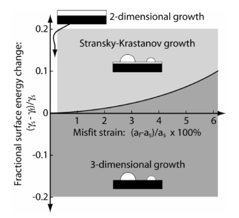
Figure 2 plots how relative surface energy change and misfit strain determine the dominant growth method.
This project is motivated by the desire to understand and predict formation of strain-relieving defects during growth of thin films. In order to accurately simulate this effect, it will be necessary to use an off-lattice, Kinetic Monte Carlo (KMC) algorithm. Relative lattice parameters will be varied.